
Battery life is a requirement like any other, so it gets tested like any other: put the device on the Hardware-in-the-Loop (HiL) rig, command it into deep sleep, read the current. The number comes back at 2.1 µA, the spec says 5 µA, the test goes green.
Six months later the field units are dead in half the predicted time.
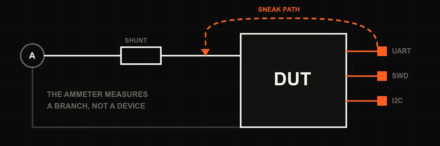
The problem is rarely the firmware. It is that a HiL fixture is, by design, a device with a dozen wires bolted to it (debug probe, serial console, bus interfaces, stimulus lines, scope probes), and every one of those wires is a conductor that can carry current into or out of the device under test (DUT). Your ammeter does not measure the DUT. It measures one branch. Everything that flows through a different branch is invisible to it.
What makes this class of bug nasty is its sign. Current injected into the DUT through a signal pin reduces what the supply has to deliver, so the measurement reads low and the test passes. A measurement that reads too high gets investigated; one that reads too low gets shipped.
The model: your ammeter measures a branch, not a device
Treat the DUT as a node and apply Kirchhoff's current law. The supply current your shunt sees is only equal to the DUT's actual consumption if the power rail and the ground return are the only conductive paths to the outside world.
                    ┌──── shunt ────┐
     Supply ────────┤               ├────── VDD ──┐
                    └───────────────┘             │
                                                  │  ← current injected here
     Debug probe ──── SWDIO / SWCLK ──────────────┤     is never seen by the shunt
     USB-UART    ──── TX / RX / RTS# ─────────────┤
     Fixture I/O ──── I2C pull-ups, CS#, CAN ─────┤
     Scope        ─── probe ground clip ──────────┤
                                                  │
     Supply GND ──────────────────────────────────┘
                         ↑
              a second ground path here bypasses
              a low-side shunt entirely
Two failure directions follow from this:
- Injection (back-powering). An external driver holds a pin above the DUT's VDD. Current flows through the pin's ESD clamp diode into the VDD net. With a high-side shunt this current substitutes for supply current and the reading drops. With a good bench supply that cannot sink, it can even go negative. Worse, the DUT may not actually be off. Its rail sits at 2.4 V instead of 0 V, RAM keeps its contents, the brown-out reset never trips, and your "cold boot after power cycle" test has been testing a warm boot for a year.
- Extraction. The DUT sources or sinks current through a pin into the fixture: driving a line high into a pull-down, holding an open-drain line low against a pull-up, charging cable capacitance at every edge. This current does come through the shunt, so the reading is inflated. Annoying, but at least it fails loudly.
Both errors are measured in tens or hundreds of microamps. Modern deep-sleep currents are 1 to 10 µA. The fixture is routinely two orders of magnitude larger than the thing you are trying to measure.
Where the shunt sits decides which mistakes are possible
Low-side sensing (shunt in the DUT's ground return) is convenient because the amplifier works near ground. It is also the wrong choice for a HiL rig. Every additional ground connection is a parallel return path around your shunt: the debug probe's ground, the USB-UART adapter's ground, the mains earth of an oscilloscope. The return current splits between the shunt and a 50 mΩ ground braid, and you measure whatever fraction happened to take your route.
High-side sensing removes the ground-loop problem but not the injection problem: current entering VDD through a signal pin still bypasses the shunt.
There is no topology that saves you. Either way, the fix is at the fixture level: control what the other wires are doing.
UART: the most under-estimated offender
The serial console is usually the first thing connected and the last thing anyone suspects. It is two wires and it has no state, so it feels harmless. It is not. A UART line is never idle in the electrical sense. It is parked at a voltage, continuously, for the entire duration of your measurement.
Which level is "idle" depends on the layer, and it matters
- TTL/CMOS UART (what you actually have between an MCU pin and a USB-serial adapter) idles high, at the I/O rail voltage. Logic 1 is the mark state. The start bit pulls the line low, so data activity is a departure downward from a permanently high line.
- RS-232 inverts this: mark (logic 1, idle) is a negative voltage, space (logic 0) is positive. This is the "active low" convention people remember, and it is the reason a transceiver sits between the two worlds.
- Modem control lines are genuinely active low: RTS#, CTS#, DTR#, DSR#, DCD#. An adapter asserts them by pulling them down, and many drivers assert DTR#/RTS# automatically when a host application opens the port.
- A break condition is the line held in the space state (low on TTL) for longer than one frame. A disconnected or unpowered transmitter can look exactly like a permanent break.
So for a low-power measurement, the question is never "how much traffic is on the console". It is: what voltage is each of these five wires sitting at while the DUT sleeps, and where does that voltage come from?
The classic: a 5 V adapter on a 3.3 V DUT
An FT232R or CH340 cable configured for 5 V I/O parks its TX output at 5 V. The DUT's RX pin has an ESD clamp diode to its own VDD. As soon as the pin voltage exceeds VDD by a forward drop, that diode conducts:
- DUT running at 3.3 V: the clamp sees roughly 5 − 3.3 − 0.7 ≈ 1 V across the driver's output impedance. With no series resistor, that is easily 10 to 20 mA flowing into the 3.3 V rail. This is above the per-pin injected-current limit of most MCUs (STM32 parts specify ±5 mA per pin, ±25 mA total), and on many devices injected current on one pin also corrupts ADC conversions on neighbouring pins, a fault that shows up as an unrelated analog test failing intermittently.
- DUT powered down: the same path now feeds the entire VDD net through one pin. Decoupling caps charge, the rail floats up to 3 or 4 V, and the DUT half-runs. Current consumption is nonsense, and so is any test that assumes a genuine power cycle happened.
Even a correctly matched 3.3 V adapter is not automatically safe. If the DUT's I/O rail is separately switched (an MCU that drops its I/O domain to 1.8 V in a low-power mode, or a board that gates a peripheral rail), a 3.3 V idle-high line is once again above VDD.
The reverse direction: the DUT paying for the console
Now the DUT's TX pin. It idles high at 3.3 V, driving into whatever the fixture put on that node:
- A 10 kΩ pull-down on the fixture side, a common "define the level so nothing floats" measure, costs 3.3 V / 10 kΩ = 330 µA, continuously. Against an STM32 standby current of about 2 µA, that is a 150× error, and it is present for the entire measurement window whether or not a single byte is transmitted.
- An unpowered adapter on the other end is worse: the DUT's high output feeds through the adapter's input clamp into the adapter's dead supply rail. Now the DUT is powering the USB-serial chip.
- Cable and receiver capacitance turn traffic into current. I = C · V · f. A metre of ribbon plus a receiver input is easily 150 pF; at 1 Mbaud with roughly one transition every two bits, that is 150 pF × 3.3 V × 500 kHz ≈ 250 µA of dynamic current, on top of the driver's own switching. If your test logs while it measures, you are measuring the log.
The control lines that reset your DUT
DTR# and RTS# deserve their own warning, because they do more than draw current. The standard ESP32 auto-reset circuit uses DTR#/RTS# to drive EN and IO0; countless custom boards copy the idea. These lines are active low, and they get asserted by any host that opens the serial port: a monitoring script, a screen session, an automatic udev rule, a Python test harness reconnecting after a timeout.
The observable symptom is a DUT that resets, or enters bootloader mode, in the middle of a measurement, for reasons that appear nowhere in the test log. Meanwhile the assertion is also a low-impedance path pulling a pulled-up reset net down, sinking the pull-up current from the DUT's rail for as long as it is held.
What to do about the console
- Match the I/O voltage properly, and match it to the lowest rail the DUT will reach during the test, not its nominal one.
- Put series resistors (1 to 10 kΩ) in every line. They do not eliminate injection. They bound it to a computable value and keep it below the datasheet's injection limit, which turns damage and unpredictability into a known error term.
- Disconnect, don't just quiet. For a genuine sleep-current measurement, open the console lines with a reed relay or a bus switch powered from the DUT rail. A line that is physically open cannot inject.
- Have the firmware cooperate. Before entering the low-power state, the DUT should drive TX to a defined level or configure it as an input with a defined pull, and it must not leave the RX pin floating: a CMOS input parked near VDD/2 turns on both transistors of the input buffer and burns tens of microamps in crowbar current all by itself.
- Stop logging inside the measurement window. Buffer diagnostics and flush them after the window closes.
JTAG and SWD: the interface that changes the answer
If UART is under-estimated, the debug port is actively misleading. It corrupts the measurement through three independent mechanisms.
1. The mandated pull-ups are a permanent load
IEEE 1149.1 requires the TAP to hold TMS and TDI (and TRST# where implemented) high when undriven, so devices implement on-die pull-ups, typically 20 to 100 kΩ. ARM's SWD equivalent puts a pull-up on SWDIO and a pull-down on SWCLK.
That is a resistor from VDD to the pin, on the DUT's own supply. If the attached probe parks those lines low when idle, each pin sinks current out of the DUT rail through the shunt. Many probes do exactly that, because "idle low" is a perfectly reasonable default when nobody is thinking about microamps:
3.3 V / 40 kΩ ≈ 82 µA per pin. Two pins held low is roughly 165 µA of pure fixture artefact, in the direction that inflates your reading.
The mirror image applies to the target reset line. nRESET is open-drain with a 10 kΩ external pull-up; a probe asserting it low draws 330 µA and holds the DUT in a state that is not the one you meant to measure.
2. The debug logic itself keeps the chip awake
This is the mechanism that produces order-of-magnitude errors, and it has nothing to do with wires at all. It is silicon that is powered because a probe is attached.
- On STM32, the DBGMCU registers (
DBG_SLEEP,DBG_STOP,DBG_STANDBY) keep HCLK and the core domain alive in low-power modes so the debugger can stay connected. A part specified at ~2 µA in standby will sit at roughly 1 mA with those bits set. Debug toolchains set them routinely, and they survive a soft reset. - On nRF52/nRF53, an attached and powered debug interface prevents genuine System OFF. The device enters an emulated equivalent instead, and the difference is roughly 0.3 µA versus over 1 mA, a factor of several thousand.
- Vendor low-power debug features, ETM/ITM trace units, and DWT cycle counters all draw current whenever they are enabled.
- SWO or TPIU trace output is a pin toggling at megahertz into cable capacitance for the entire session. That is dynamic current attributable purely to observation.
And there is a measurement-methodology point underneath: a halted core has a completely different current profile from a running one. Breakpoints, single-stepping and memory reads through the DAP all perturb exactly the thing under test.
The only reliable answer is to detach the debugger for power measurements: power the probe down, tri-state its lines, or physically open them with relays. Verify as well that the DBGMCU-equivalent bits are cleared by a full power cycle before the measurement window opens. If your HiL sequence flashes firmware and then measures without a power cycle in between, it is measuring the debug session.
3. VTREF, target power and boundary scan
- Most probes sense the target I/O voltage on VTREF to set their level shifters. Check that this pin is genuinely high-impedance on your probe; some cheap clones drive their translators from their own supply and feed current back into the target rail through it.
- Several probe headers carry an optional target power output (a switchable 3.3 V or 5 V pin). Enabled by accident, it supplies the DUT in parallel with your metered supply and the measurement is meaningless.
- Boundary scan EXTEST literally drives the DUT's pins from the probe. Useful for interconnect testing, catastrophic if it is still active when you take a current reading.
- Adaptive clocking (RTCK) adds one more continuously driven line to the budget.
The rest of the usual suspects
The same two mechanisms reappear on every other interface: a parked voltage that drives current, and a conductive path that bypasses the shunt.
I²C. Open-drain plus pull-ups, so the location of those pull-ups decides everything. If they live on the fixture and are tied to a fixture rail, an unpowered DUT gets back-powered through both pins. If they live on the DUT, a fixture master holding SDA or SCL low (a stuck bus, an aborted transfer, or a master that clock-stretches) sinks 3.3 V / 4.7 kΩ ≈ 700 µA per line out of the DUT's supply. An idle bus is high and costs nothing, which is exactly why the failure only appears when something goes wrong elsewhere.
SPI. CS# is active low and idles high; SCLK and MOSI idle at whatever the master left them. Every one of those is a driven line into the DUT. If the fixture master is powered down while the DUT is not, the DUT's MISO output feeds the master's clamps instead.
CAN. A dominant bit drives roughly 2 V across a 60 Ω terminated bus, which is about 33 mA from the DUT's supply plus transceiver quiescent current. A HiL rig that keeps background bus traffic running during a sleep-current test is not measuring sleep. Split termination biased from a fixture rail back-powers the transceiver when the DUT is off, and the transceiver's own standby pin (usually an active-low STB#) must be in the state the product actually ships with. LIN is the same story with a 1 kΩ master pull-up to 12 V, so a dominant level costs about 12 mA.
USB. VBUS is a second power source, full stop. A self-powered design still needs to prove it does not draw from it. Even with no traffic, the 1.5 kΩ D+ pull-up against the host's 15 kΩ pull-down draws roughly 200 µA continuously just to signal that a device is present, and keeping the PHY's 48 MHz clock alive costs milliamps.
Fixture I/O in general. Presence-detect and ID lines pulled up from the fixture; opto-coupler inputs whose LED current comes from the DUT (milliamps, by construction); LEDs on the fixture driven by DUT outputs; ADC stimulus sources that remain connected and drive current into an analog input through its clamp; boot-strap pins held by the fixture.
Instruments. A 10:1 scope probe is 10 MΩ and draws nothing worth mentioning, but its ground clip ties the DUT to mains earth, creating a parallel return path that quietly bypasses a low-side shunt and adds a ground loop. Prefer differential probes or an isolated scope on a low-power fixture.
The fixture's own leakage. At the microamp level, hardware you consider passive stops being passive. Solid-state relays leak microamps when off; analog muxes leak nanoamps at 25 °C and hundreds of nanoamps at 85 °C; unwashed flux residue and humidity make a PCB surface conduct measurably. This is why the fixture baseline must be re-verified over time and not assumed.
Building a fixture that does not lie
Ranked roughly by how much they actually help:
- Physically disconnect during the measurement window. Reed relays on every peripheral line: console, debug, buses, stimulus. Nothing beats an open circuit, and it is the only approach that scales down to single-digit microamps.
- Power the fixture-side interface from the DUT's own rail. Level shifters and bus switches (TS3A/NX3L/FSA-class) whose supply is the DUT rail stop driving when the DUT rail collapses, so back-powering disappears by construction. Verify the specific part does not back-feed through its own supply pin.
- Drive OE explicitly. Prefer translators with an output-enable over auto-direction-sensing parts, and let the test sequencer own that signal rather than leaving it strapped active.
- Series resistance everywhere. 1 to 10 kΩ in every fixture-to-DUT signal line. It bounds injection to a computable value and protects the pin.
- Isolate where the topology allows it. Digital isolators or an isolated USB-UART remove the ground loop. Be honest about the trade-off: an isolator's DUT-side supply is itself a milliamp-class load, so it belongs on a rail outside the measurement, not on the metered one.
- Make the measurement window a first-class concept in the test framework. A single state that stops logging, quiets the buses, tri-states drivers, opens relays, settles, measures, then restores. Not a
sleep()and a hope. - Choose the instrument for the job. A bench DMM in current mode has hundreds of millivolts of burden voltage on its microamp ranges, enough to brown out the DUT on a wake-up spike, and its auto-ranging blinds it for tens of milliseconds exactly when the interesting transient occurs. Use a source-measure unit or a power analyser with fast, seamless ranging.
Four checks that catch all of this
1. The dark test. Bring the fixture up in its normal idle state, then remove DUT power at the shunt. Measure the current at the DUT's power pins, and measure the voltage on the DUT's VDD node. Both should be zero. Any current above your noise floor, or any rail sitting at 2.7 V with the supply off, is injection. You now know it exists before it has corrupted a single test result. Run this at the start of every campaign.
2. Cable-by-cable delta budget. Measure the bare board on a clean supply with nothing else attached. Then attach one harness at a time and record the delta. The result is a table like this, and it is your fixture's error budget:
| Connection | Δ sleep current | Cause |
|---|---|---|
| Bare DUT | 2.1 µA | reference |
| + USB-UART (3.3 V, 10 kΩ pull-down) | +330 µA | TX idle high into pull-down |
| + SWD probe attached, idle low | +165 µA | on-die TMS/TDI pull-ups |
| + SWD probe, debug session active | +1.1 mA | DBGMCU keeps core clocked |
| + I²C fixture pull-ups | +0 µA (idle) / +700 µA (stuck low) | state-dependent |
3. Compare against a golden reference. Battery, bare board, no fixture, a known firmware image. Any HiL number that cannot be reconciled with the reference is a fixture number, not a product number.
4. State the uncertainty in the report. If the requirement is 5 µA, the fixture's own contribution needs to be an order of magnitude below that, and the test report should say what it was. "Measured 2.1 µA" is not a result; "measured 2.1 µA with a verified fixture contribution below 0.2 µA" is.
Conclusion
A HiL rig is built to observe a device, and observation costs current. That cost is not small. The routine mistakes sit between 100 µA and 1 mA against sleep currents of a few microamps: an idle-high TX line into a pull-down, a debug probe parking its lines low, a debug session that keeps the core clocked, a second ground path around a low-side shunt.
The dangerous half of these errors point downward, making the DUT look more efficient than it is, so they pass the test and surface later as warranty returns. Treat the fixture as part of the measurement chain: characterise its contribution, disconnect what you can during the measurement window, and re-run the dark test regularly. A power number from a HiL rig is only trustworthy once you can say what the rig itself was drawing.